Functional safety of electrical/electronic/programmable electronic safety-related systems –
Part 2: Requirements for electrical/electronic/programmable electronic safety-related systems
Annex E
(normative)
Special architecture requirements for integrated circuits (ICs) with on-chip redundancy
E.1General
This annex is referenced by 7.4.2.2 b).
To allow the use of on-chip redundancy for ICs with one common semi-conductor substrate, a set of requirements is given below. For safety reasons this approach has a conservative nature, for example it is limited up to SIL 3 and a set of restrictive requirements have been specified. The following requirements are related to digital ICs only. For mixed-mode and analogue ICs no general requirements can be given at the moment. Common cause analysis (see IEC 61 508-1 , 7.6.2.7) may exclude the use of on-chip redundancy for an individual application. On-chip redundancy as used in this standard means a duplication (or triplication etc.) of functional units to establish a hardware fault tolerance greater than zero. According to 7.4.4.1.1a) in determining the hardware fault tolerance no account is taken of measures that may control the effects of faults such as diagnostics.
A subsystem with a hardware fault tolerance greater than 0 can be realised using one single IC semi-conductor substrate (on-chip redundancy). In this case all of the following requirements a) to q) shall be fulfilled and the design of the E/E/PE system and the IC shall be such as to meet these requirements. An IC with on-chip redundancy shall have its own compliant item safety manual (see Annex D).
a) The highest safety integrity level that can be claimed for a safety function using an IC as described above is limited to SIL 3.
NOTE 1 At the present state of the art, knowledge and experience, it is not feasible to consider and take measures against all effects related to said element (single IC) to gain sufficient confidence for SIL 4.
b) The systematic capability shall not be increased by combination of elements (see
7.4.3.2).
c) To avoid common cause failure(s), the effects of increasing temperature, for example due to random hardware fault(s), shall be considered. At least one of the measures listed in Table E.2, no. 6 shall be applied. In a design where a local fault can cause a safety critical temperature increase, appropriate measures shall be taken.
NOTE 2 While in a power design a local fault can cause a significant temperature increase, the impact of a local short circuit in a logic circuit can be negligible.
Examples to be considered in digital circuits include the device padarea and voltage regulators.
d) Separate physical blocks on substratum of the IC shall be established for each channel and each monitoring element such as a watchdog. The blocks shall include bond wires and pin-out. Each channel shall have its own separated inputs and outputs which shall not be routed through another channel/block.
NOTE 3 This does not exclude internal connections between blocks by wiring between output and input cells of different blocks (see also Table E.1, 3a and 3b).
NOTE 4 Input and outputs include, but are not limited to:
– DFT signals (Design for Testability, e.g. scan chains);
– Clock signals and clock enable signals;
– Power supply;
– Reset signals;
– Configuration and mode selection signals;
– Debug and trace signals.
e) Appropriate measures shall be taken to avoid dangerous failure caused by faults of the power supply including common cause failures.
NOTE 5 Faults of the power supply include, but are not limited to:
– noise;
– disturbance propagation over the power supply lines;
– non-simultaneous power supply switch-on, that may cause effects such as latch-up or high in-rush current;
– excessive current-draw resulting from short circuit.
NOTE 6 This requirement can be fulfilled by applying adequate techniques such as:
– providing each block with its own power supply pins so that no block is supplied via the power supply of another block (for example via internal connections) and not connecting wells of separate physical blocks together inside the IC (see also Table E.2, no. 3);
– incorporation of external measures to avoid dangerous failures that may be caused by different voltages of the
wells;
– detecting power supply faults by means of voltage monitors;
– using partially increased voltage tolerance;
– considering IR drop problems for the design of power lines.
f) The minimum distance between boundaries of separate physical blocks shall be sufficient to avoid short circuit and cross talk between these blocks.
NOTE 7 Short circuit typically can be caused by electro migration, via migration, contact migration, local defect gate oxide breakdown, latch-up, etc.
NOTE 8 Cross talk typically can be caused by substrate currents, capacitive coupling, etc.
NOTE 9 The minimum distance should be chosen regarding the relevant design rules with a safety factor typically between 1 0 and 50.
NOTE 1 0 Potential rings according to Table E.2 are not considered as being part of a block when estimating the distance between separate physical blocks.
g) Short circuit and/or cross-talk between adjacent lines of separate physical blocks shallnot lead to a loss of a safety function or an undetected loss of a monitoring function (Table E.2, no. 5).
h) substratum shall be connected to ground whatever the IC design process used (n-well orp-well);
NOTE 1 1 For p-wells, this means the use of a negative power supply. Negative logic should be avoided since its use may be susceptible to errors in design.
i) The susceptibility of an IC with on-chip redundancy to common cause failures shall be estimated by determining a β-factor according to E.3. This β-factor called β IC shall be used when estimating the achieved safety integrity of the E/E/PE safety-related system according to 7.4.5.1and will be used for the IC instead of the β-factor determined for example according to Annex D of IEC 61 508-6.
j) The detection of a fault (by diagnostic tests, proof tests or by any other means) in an IC with on-chip redundancy shall result in a specified action to achieve or maintain a safe state.
NOTE 1 2 This requirement does not apply, if the effects of a fault can be controlled, for example by de- energization of a block.
k) The minimum diagnostic coverage of each channel shall be at least 60 %. Where a
monitoring element is implemented only once, the minimum diagnostic coverage for this element shall also be at least 60 %.
l) If it is necessary to implement a watchdog, for example for program sequence monitoringand/or to guarantee the required diagnostic coverage or safe failure fraction one channel shall not be used as a watchdog of another channel, except when functionally diverse channels are used.
m) When testing for electromagnetic compatibility without additional safety margin, the function carried out by the IC shall not be interfered (for example performance criterion A as described in EMC immunity standards, see for example IEC 61 000-6-2 or IEC 61 326- 3-1 ).
n) When testing for electromagnetic compatibility with additional safety margins, the safety function (including IC) shall comply with the “FS” criterion as defined in IEC 61 326-3-1
o) Appropriate measures shall be taken to avoid dangerous failure caused by oscillations of digital input ports connected to external asynchronous digital signals, e.g. introduction of respective multiple clock synchronization stages.
p) The common cause potential of common resources such as boundary scan circuitries andarrays of special function registers shall be analyzed.
q) The requirements a) to p) list common cause initiators specific to ICs with on-chip redundancy. Other relevant common cause initiators shall be considered as specified in this International Standard.
NOTE 1 3 In general the above requirements restrict the use of on-chip redundancy to ICs designed with a full-custom or semi-custom approach such as ASICs, microcontrollers or other specialised SoCs (systems on chip).
Other designs such as Gate Arrays, FPGAs etc. may not meet all requirements.
Use of ICs with on-chip redundancy as described above shall only be permitted if a full common cause analysis (CCA) has been undertaken. This analysis shall cover the complete range of potential common cause failures arising from design, fabrication, construction, procedural and environmental factors. In particular, the loss of physical separation between channels as a result of the use of ICs with on-chip redundancy shall be subject to special scrutiny. The final SIL level assigned to the E/E/PE safety-related system shall be dependent upon the results of this CCA.
NOTE 1 4 The use of physical separation (i.e. segregation) of “channels” can provide defence against a widerange of common mode failures in redundant systems.
NOTE 1 5 The CCA methodology proposed is structured into the following steps:
1 . Identify potential common cause initiators (CCI). Consider effects listed in this annex and other foreseeable physical CCI and logical CCI (shared resources and signals).
2. Identify the redundant blocks on the IC which will suffer from CCI amongst them.
3. Qualitatively list and evaluate the safety measures against the individual CCI identified in step 1 for eachpair of redundant blocks identified in step 2.
4. Quantitatively answer the Tables E.1and E.2 for each pair of redundant blocks identified in step 2 and evaluate the specific ß factor.
5. Use the specific ß factors in the probabilistic modelling.
E.2 Additional requirements for SIL 3 on-chip redundancy
For SIL 3 on-chip redundancy the following requirements shall be met in addition to the requirements given in E.1:
a) documented evidence that all application specific environmental conditions are in
accordance with that taken into account during specification, analysis, verification and validation shall be provided;
b) external measures that can achieve or maintain a safe state of the E/E/PE system. These measures shall achieve medium effectiveness (see also A.3) as minimum. All measures implemented inside the IC to monitor for effects of systematic and/or common cause failures shall use these external measures to achieve or maintain a safe state of the E/E/PE system.
E.3 β-factor
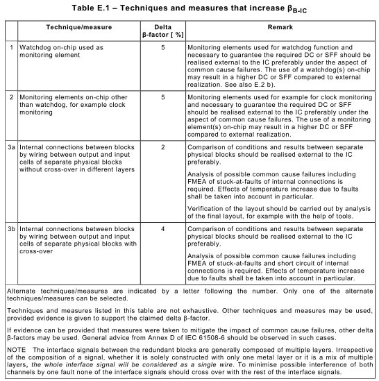
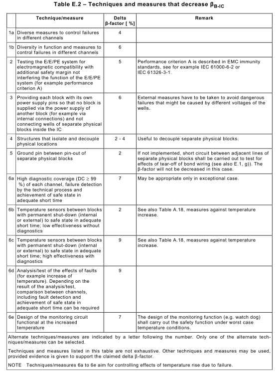
The susceptibility of the IC with on-chip redundancy to common cause failures shall be estimated by determining the β-factor β IC , which is special to ICs with on-chip redundancy (see also E.1, i)). The estimation shall be based upon the following:
a) a basic β-factor called β B-IC of 33 %;
b) estimation of the increase of the basic β-factor, β B-IC , by the design using Table E.1; and
c) estimation of the decrease of the basic β-factor, β B-IC , by the design using Table E.2.
β IC is estimated by adding β B-IC and all scores from Table E.1and afterwards subtracting all scores from Table E.2. The estimated final β IC shall not exceed 25 %.
NOTE 1 This β-factor called β IC will be used when estimating the achieved safety integrity of the E/E/PE safety-related system according to 7.4.5.1and will be used for the IC instead of the β-factor determined for example according to Annex D of IEC 61 508-6.
NOTE 2 A specific analysis of the available failure data for the IC design methodology applied should be undertaken to substantiate that the chosen β-factor is conservative. Only ICs with mature design and implementation processes should be used.